Anyone milling PCBs?
2015-12-31 by me@...
Yahoo Groups archive
Index last updated: 2026-04-28 23:05 UTC
Thread
2015-12-31 by me@...
2015-12-31 by Cristian
At 06:22 PM 31-12-15, you wrote:
>
>
>Is anyone out there milling PCBs?    My new CNC 3020 is on its way
>along with an Arduino controller and I have a number of
>questions.   Before I post them just wanted to make sure I am in the
>right place. :)

I do.
Cristian
2015-12-31 by Dave Wade
Built a milling attachment for my 3D printer but not yet made any PCBs. Been looking at a CNC3040 so me interested to hear how you get on…

Dave
G4UGM

From: Homebrew_PCBs@yahoogroups.com [mailto:Homebrew_PCBs@yahoogroups.com]
Sent: 31 December 2015 16:23
To: Homebrew_PCBs@...m
Subject: [Homebrew_PCBs] Anyone milling PCBs?


Is anyone out there milling PCBs?    My new CNC 3020 is on its way along with an Arduino controller and I have a number of questions.   Before I post them just wanted to make sure I am in the right place. :)
2015-12-31 by Boots Hughston
I have been milling pc's for 3 or 4 years

Boots-2b1

Sent from my iPhone
> On Dec 31, 2015, at 8:22 AM, me@... [Homebrew_PCBs] <Homebrew_PCBs@yahoogroups.com> wrote:
>
> Is anyone out there milling PCBs?    My new CNC 3020 is on its way along with an Arduino controller and I have a number of questions.   Before I post them just wanted to make sure I am in the right place. :)
>
>
>
>
2015-12-31 by me@...
2015-12-31 by me@...
2016-01-02 by Bob Butcher
2016-01-02 by me@...
2016-01-03 by Harvey White
On 31 Dec 2015 13:15:11 -0800, you wrote:

>Didn't see my post maybe there is a delay?   Anyway I will restate my questions since they are open to everyone.
>
>What software to use to control the mill?  I considered Mach3 but it has two problems.   First it only works with a parallel port from what I understand.

TurboCNC also works with a parallel port in a minimal (DOS)
environment.  Don't use it in a DOS window under windows.

>I need USB.

USB has no guaranteed delivery time, and sends when the CPU gets
around to it.

>From what I understand there are USB controllers that might work with mach3?   But most important the Free version of Mach3 is really limited on the steps it can process.

The reason for a USB controller is to generate the pulses in hardware
that is not subject to a windows/linux operating system timing.  All
the USB does is download commands, the pulses are generated locally.


>
>I figure I will use one of those Arduino controllers.   Already have one on order.  I thought I would use Universal GCode Sender.   Are there better affordable options?

No idea, I've messed with rolling my own, using an FPGA for timing. In
theory, it works well.  Haven't managed to get the hardware working
(mill, etc.) quite yet.  Too many other things.

The standalone controllers include Gcode interpreters, so yes, the
Arduino approach should work well.  Don't know about Universal Gcode
Sender.

Harvey
2016-01-03 by keith printy
If you are using a desktop pc ,you could always install a parallel port. I
have an old laser printer that required one and all I had was usb. The board
I installed also gave me serial ports and was maybe about $30
From: Homebrew_PCBs@yahoogroups.com [mailto:Homebrew_PCBs@yahoogroups.com]
Sent: Sunday, January 03, 2016 9:43 AM
To: Homebrew_PCBs@yahoogroups.com
Subject: Re: [Homebrew_PCBs] Re: Anyone milling PCBs?


On 31 Dec 2015 13:15:11 -0800, you wrote:


>Didn't see my post maybe there is a delay? Anyway I will restate my
questions since they are open to everyone.
>
>What software to use to control the mill? I considered Mach3 but it has two
problems. First it only works with a parallel port from what I understand.


TurboCNC also works with a parallel port in a minimal (DOS)
environment. Don't use it in a DOS window under windows.


>I need USB.


USB has no guaranteed delivery time, and sends when the CPU gets
around to it.


>From what I understand there are USB controllers that might work with
mach3? But most important the Free version of Mach3 is really limited on the
steps it can process.


The reason for a USB controller is to generate the pulses in hardware
that is not subject to a windows/linux operating system timing. All
the USB does is download commands, the pulses are generated locally.


>
>I figure I will use one of those Arduino controllers. Already have one on
order. I thought I would use Universal GCode Sender. Are there better
affordable options?


No idea, I've messed with rolling my own, using an FPGA for timing. In
theory, it works well. Haven't managed to get the hardware working
(mill, etc.) quite yet. Too many other things.


The standalone controllers include Gcode interpreters, so yes, the
Arduino approach should work well. Don't know about Universal Gcode
Sender.


Harvey
2016-01-03 by Bob Butcher
I purchased BobCad CAM a couple of years ago, and find it very helpful. All you need to do is define the origin when starting a layout (I use the left rear corner of the board) and move your tool to that position and set X & Y to zero. BobCad CAM is quite expensive (I paid $800), but I do quite a bit of CNC machining in metal as well, so it does save a lot of time. I am using Mach3 to run my milling machine, and BobCad CAM has a post processor that makes it easy to create GCode files. BobCad CAM allows you to chose a toolpath and a tool and if you need to change tools, you can add a few lines of code to the NC file to remind you to change tools at the correct time. Mach3 does include a CAM converter called EasyCam, but I have not tried it. There is a learning curve to using the software, but that is always true to some extent. Before I purchased BobCad and Mach3, I used a JAVA program that I wrote to convert DXF files to native Galil code which I could run using my Galil DMC 1850 interface board in my PC. It was quite time consuming to do this conversion,. but it did work most of the time.
For very simple boards you could probably manually write your own GCode, but that will sometimes lead to errors and broken tools or destroyed boards when you make a mistake.
If you have a program to create DXF files of the layout, you can open them in any program that reads text and extract the co-ordinates easily (well maybe not so easily). Try opening a DXF file sometime and search for ENTITIES. The text following that keyword has all the information you need, but it can be a bit of a job to interpret. For example a series of lines reading:LINE  56E03301F100AcDbEntity  8ROW1100AcDbLine 10-0.1750000000000043 201.830865704890999 300.0 11-0.1750000000000131 213.136198601993994 310.0  0
First this is a line. The layer is ROW1 if you care. The number 10 means the next line of data contains the starting X value,
The number 20 means the next line of data contains the starting Y value, The number 30 means the next line of data contains the starting Z value. The number 11 means the next line of data contains the ending X value, The number 21 means the next line of data contains the ending Y value, The number 31 means the next line of data contains the ending Z value. So this is a line from point -0.1750000000000043, 1.830865704890999, 0.0 to -0.1750000000000131, 3.136198601993994, 0.0The final entry of zero indented one space means the end of that entity.
Circles and Arcs get kind of weird, since the DXF standard uses starting point, radius, and bulge to define am arc. I avoid curved lines and pads in my layout when trying to interpret DXF files.
If you really want to pursue this subject, you can Google DXF and find the protocol used to define various items.
Another potential (or real) problem is the DXF file lists the entities in the order drawn in your CAD program, so any motion may not be optimized very well. Another pitfall in hand coding is that you need to manually determine when to raise and lower the tool. Typically I lower the tool and cut a full island, then raise the tool for the move to the next island start.
2016-01-03 by Bob Butcher
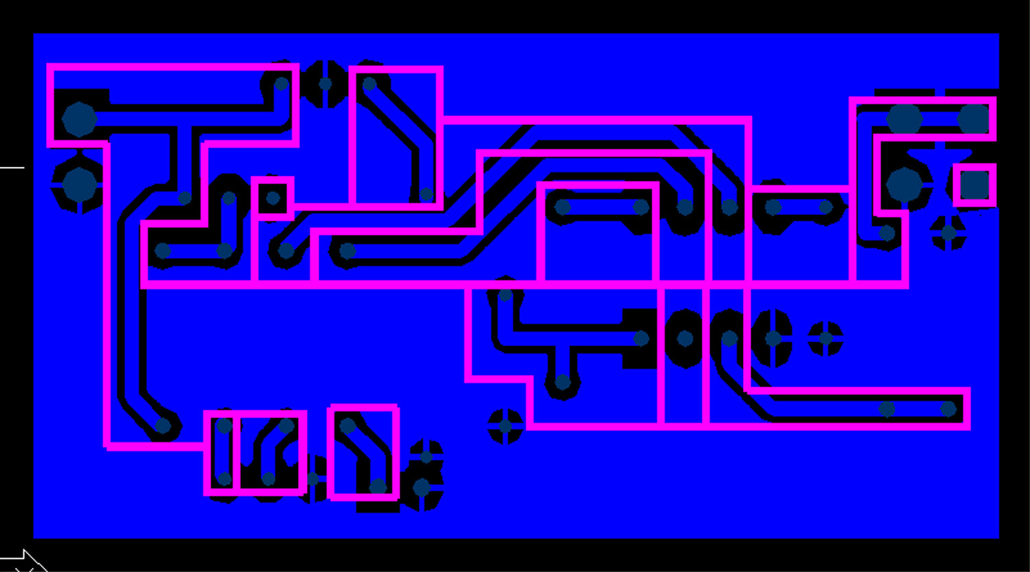
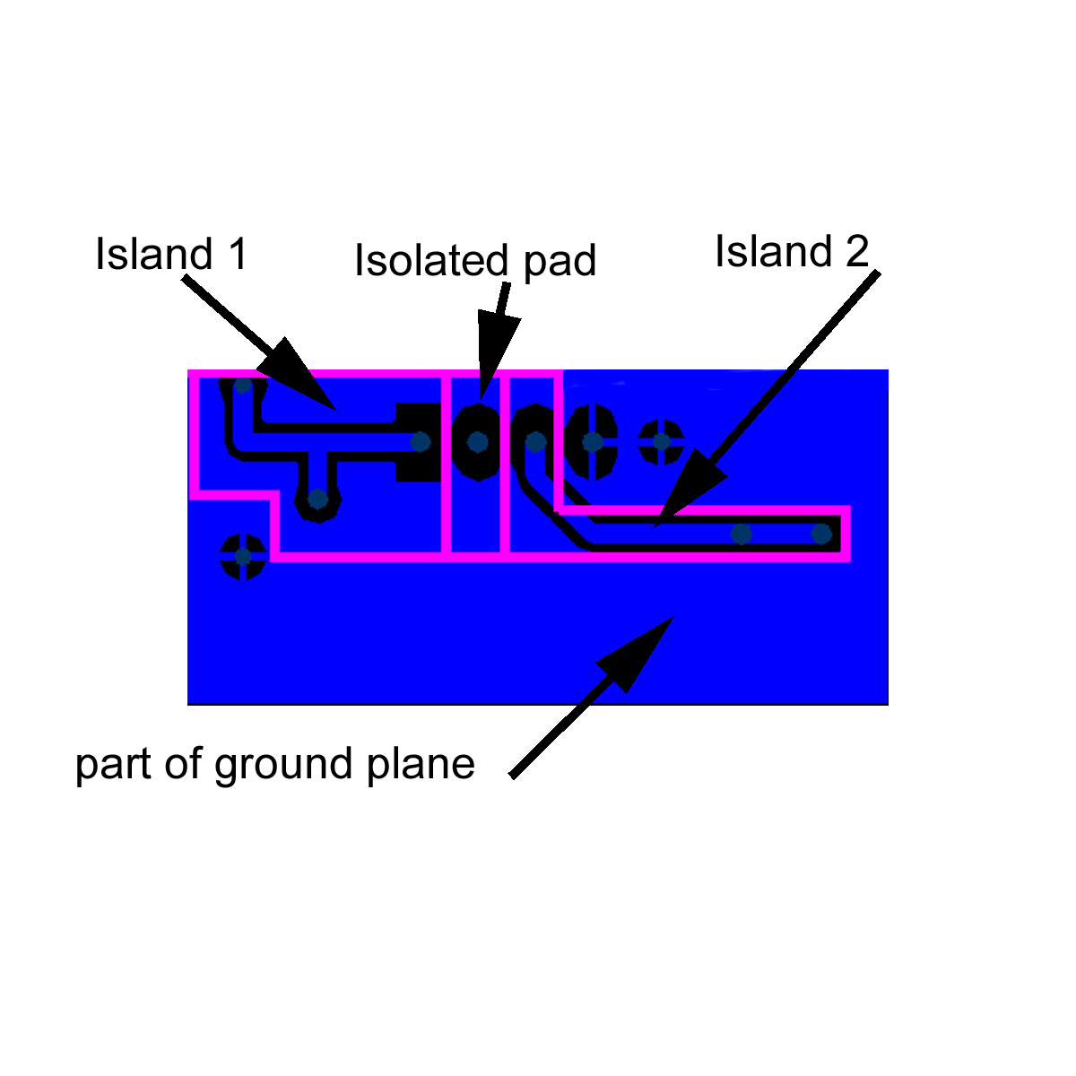
If you open the attached PCB you will see a group of pads connected by traces (all blue). All the pads are outlined by rectangles, and lines are then used to join all the rectangles that are connected by copper. The lines and rectangles are then trimmed to create an "island" that contains all the copper that is connected together. The attached image shows an example, and is part of the board shown on the last e-mail. Please note if you look carefully at the full board, there is an error where an island has a missing pink line, allowing it to connect to the ground plane.
This is only one layer of the PCB, the bottom layer in this case. The blue area is the copper on the layer as designed with the PCBlayout program. The black lines are where the copper would be removed if the board was etched at a PCB fab shop. The dark grey dots are pads that would have a hole drilled through the board for mounting a component or connecting a wire. The pink lines are the lines that will be cut by my CNC machine, removing the copper. I would follow up by drilling holes in the pads for component mounting. Note that the area labeled Island 1 has 3 pads connected by a copper trace. When the copper is cut on the pink lines, the three pads are isolated from the rest of the copper just as if it were cut on the black lines. I could have used the CNC to cut on all the black lines, but that would take more time and might not leave enough copper for the trace, perhaps causing it to lift from the board from the cutting forces. The region labeled Island 2 also contains 3 pads. The region labeled Isolated pad has only 1 pad, which has no connections on this layer. It may have a connection on the top layer (not shown), or it may be an unused pin on some component. The bulk of the blue area is ground plane, only part of it shown on this example. The ground plane connects all the pads on the board that are connected to ground.
The top layer of the board may also have a pattern connecting pads, or perhaps this is a single layer board. Note that if it is a double layer PCB, and if any pads connect to both top and bottom layers, the wire or component lead must be soldered to both sides of the board. Sometimes it is necessary to use a VIA to connect top and bottom layers, which would be done with a plated through hole if built by a PCB fab shop. Since I do not have plated through hole capability, I install a wire and solder it to both layers, unless it is a lead on a component that is not hidden underneath the component.
I generally like to use surface mount components for as much of the design as possible since there are less holes to drill. I usually hand solder the components onto the board since I do not have solder mask capability. To avoid future corrosion problems I generally use flux and solder coat the entire copper area of the board before adding components and wires. Of course you need to check all the cuts to make sure you do not have a solder bridge or copper whisker shorting adjacent islands before adding components.
It is always a good idea to consider how the board will be soldered when performing the PCB layout since it can be difficult or impossible to solder wires or leads to the pad if the pads are located under a component, so I try to design all my boards to use vias located outside the component for these connections. Sometimes vias can be located under a component, but a wire must be soldered to both layers before the component is placed on the board. If this does not make sense now, it will become more obvious when you actually build a few boards.  It is also good to remember when laying out the board that metal cases on components may short to the bare metal underneath since there is no solder mask.
Note that I tend to leave as much copper as possible on the board, and only remove it where needed to isolate pads. This makes it much easier to machine the cuts, and if you are etching the board, it requires less etchant and less time to remove copper.
I hope this answers your questions.
Bob
2016-01-03 by Aaron Turner
I purchased BobCad CAM a couple of years ago, and find it very helpful. All you need to do is define the origin when starting a layout (I use the left rear corner of the board) and move your tool to that position and set X & Y to zero. BobCad CAM is quite expensive (I paid $800), but I do quite a bit of CNC machining in metal as well, so it does save a lot of time. I am using Mach3 to run my milling machine, and BobCad CAM has a post processor that makes it easy to create GCode files. BobCad CAM allows you to chose a toolpath and a tool and if you need to change tools, you can add a few lines of code to the NC file to remind you to change tools at the correct time. Mach3 does include a CAM converter called EasyCam, but I have not tried it. There is a learning curve to using the software, but that is always true to some extent.Before I purchased BobCad and Mach3, I used a JAVA program that I wrote to convert DXF files to native Galil code which I could run using my Galil DMC 1850 interface board in my PC. It was quite time consuming to do this conversion,. but it did work most of the time.For very simple boards you could probably manually write your own GCode, but that will sometimes lead to errors and broken tools or destroyed boards when you make a mistake.If you have a program to create DXF files of the layout, you can open them in any program that reads text and extract the co-ordinates easily (well maybe not so easily). Try opening a DXF file sometime and search for ENTITIES. The text following that keyword has all the information you need, but it can be a bit of a job to interpret. For example a series of lines reading:LINE56E03301F100AcDbEntity8ROW1100AcDbLine10-0.1750000000000043201.830865704890999300.011-0.1750000000000131213.136198601993994310.00First this is a line. The layer is ROW1 if you care. The number 10 means the next line of data contains the starting X value,The number 20 means the next line of data contains the starting Y value, The number 30 means the next line of data contains the starting Z value. The number 11 means the next line of data contains the ending X value,The number 21 means the next line of data contains the ending Y value, The number 31 means the next line of data contains the ending Z value.So this is a line from point -0.1750000000000043, 1.830865704890999, 0.0 to -0.1750000000000131, 3.136198601993994, 0.0The final entry of zero indented one space means the end of that entity.Circles and Arcs get kind of weird, since the DXF standard uses starting point, radius, and bulge to define am arc. I avoid curved lines and pads in my layout when trying to interpret DXF files.If you really want to pursue this subject, you can Google DXF and find the protocol used to define various items.Another potential (or real) problem is the DXF file lists the entities in the order drawn in your CAD program, so any motion may not be optimized very well. Another pitfall in hand coding is that you need to manually determine when to raise and lower the tool. Typically I lower the tool and cut a full island, then raise the tool for the move to the next island start.
2016-01-04 by Brad Thompson
On 1/3/2016 6:05 PM, Aaron Turner synfinatic@... [Homebrew_PCBs]
wrote:
> I'm curious- has anyone tried using Fusion360 for CAD/CAM for milling
> PCB's?  I've used Fusion360 with great results for designing parts for
> my 3D printer and it includes a pretty decent CAM module I'm told.
> And unlike BobCAD, it's free if you make less then $100k/year using
> the software which makes it a great choice for non-professionals.
>
Hello--

I inquired about this topic (deposition of plastic extruded resist
directly onto copperclad board via 3-D printer) a while
ago. Has anyone recently experimented with this approach? It's the
inverse of a subtractive (milling) process,
but the CAD/CAM software should equally well apply.


Thanks, and 73--

Brad  AA1IP
2016-01-04 by Tony Smith
> On 1/3/2016 6:05 PM, Aaron Turner synfinatic@... [Homebrew_PCBs]
> wrote:
> > I'm curious- has anyone tried using Fusion360 for CAD/CAM for milling
> > PCB's?  I've used Fusion360 with great results for designing parts for
> > my 3D printer and it includes a pretty decent CAM module I'm told.
> > And unlike BobCAD, it's free if you make less then $100k/year using
> > the software which makes it a great choice for non-professionals.
> >
> Hello--
>
> I inquired about this topic (deposition of plastic extruded resist directly onto
> copperclad board via 3-D printer) a while ago. Has anyone recently
> experimented with this approach? It's the inverse of a subtractive (milling)
> process, but the CAD/CAM software should equally well apply.
>
>
> Thanks, and 73--
>
> Brad  AA1IP


I doubt it would be fine enough.  That said are people doing 3D-ish printers where they print the traces instead using that silver conductive paint or similar, so who knows.

People have tried to print either the resist or traces directly onto copper board with inkjet printers with little success.

Mark (?) on this list managed to laser print directly onto copper which surprised me.

I've been meaning to try the 'spray board with paint and laser it off' method.  Diptrace will export a file suitable for milling (isolation traces) that will work for lasering.  Should be fairly simple and fast, certainly quieter than a mill.

Tony
2016-01-04 by <n0tt1@...>
But then you have to deal with the fumes from burning paint.

73,
Charlie

On Mon, 4 Jan 2016 22:51:43 +1100 "'Tony Smith' ajsmith1968@...
[Homebrew_PCBs]" <Homebrew_PCBs@yahoogroups.com> writes:

> On 1/3/2016 6:05 PM, Aaron Turner synfinatic@... [Homebrew_PCBs]
> wrote:
> > I'm curious- has anyone tried using Fusion360 for CAD/CAM for milling
> > PCB's? I've used Fusion360 with great results for designing parts for
> > my 3D printer and it includes a pretty decent CAM module I'm told.
> > And unlike BobCAD, it's free if you make less then $100k/year using
> > the software which makes it a great choice for non-professionals.
> >
> Hello--
>
> I inquired about this topic (deposition of plastic extruded resist
directly onto
> copperclad board via 3-D printer) a while ago. Has anyone recently
> experimented with this approach? It's the inverse of a subtractive
(milling)
> process, but the CAD/CAM software should equally well apply.
>
>
> Thanks, and 73--
>
> Brad AA1IP

I doubt it would be fine enough. That said are people doing 3D-ish
printers where they print the traces instead using that silver conductive
paint or similar, so who knows.

People have tried to print either the resist or traces directly onto
copper board with inkjet printers with little success.

Mark (?) on this list managed to laser print directly onto copper which
surprised me.

I've been meaning to try the 'spray board with paint and laser it off'
method. Diptrace will export a file suitable for milling (isolation
traces) that will work for lasering. Should be fairly simple and fast,
certainly quieter than a mill.

Tony
2016-01-04 by Bob Butcher
That is a good idea. You must have at least Windows 7 and must have a 64 bit system for it to work however.
Bob

    On Sunday, January 3, 2016 4:05 PM, "Aaron Turner synfinatic@... [Homebrew_PCBs]" <Homebrew_PCBs@yahoogroups.com> wrote:


     I'm curious- has anyone tried using Fusion360 for CAD/CAM for milling PCB's?  I've used Fusion360 with great results for designing parts for my 3D printer and it includes a pretty decent CAM module I'm told.  And unlike BobCAD, it's free if you make less then $100k/year using the software which makes it a great choice for non-professionals.
--
Aaron Turner
https://synfin.net/         Twitter: @synfinatic
Those who would give up essential Liberty, to purchase a little temporary
Safety, deserve neither Liberty nor Safety.
    -- Benjamin Franklin
On Sun, Jan 3, 2016 at 11:39 AM, Bob Butcher bbutcher85@... [Homebrew_PCBs] <Homebrew_PCBs@yahoogroups.com> wrote:

      I purchased BobCad CAM a couple of years ago, and find it very helpful. All you need to do is define the origin when starting a layout (I use the left rear corner of the board) and move your tool to that position and set X & Y to zero. BobCad CAM is quite expensive (I paid $800), but I do quite a bit of CNC machining in metal as well, so it does save a lot of time. I am using Mach3 to run my milling machine, and BobCad CAM has a post processor that makes it easy to create GCode files. BobCad CAM allows you to chose a toolpath and a tool and if you need to change tools, you can add a few lines of code to the NC file to remind you to change tools at the correct time. Mach3 does include a CAM converter called EasyCam, but I have not tried it. There is a learning curve to using the software, but that is always true to some extent. Before I purchased BobCad and Mach3, I used a JAVA program that I wrote to convert DXF files to native Galil code which I could run using my Galil DMC 1850 interface board in my PC. It was quite time consuming to do this conversion,. but it did work most of the time.
For very simple boards you could probably manually write your own GCode, but that will sometimes lead to errors and broken tools or destroyed boards when you make a mistake.
If you have a program to create DXF files of the layout, you can open them in any program that reads text and extract the co-ordinates easily (well maybe not so easily). Try opening a DXF file sometime and search for ENTITIES. The text following that keyword has all the information you need, but it can be a bit of a job to interpret. For example a series of lines reading:LINE  56E03301F100AcDbEntity  8ROW1100AcDbLine 10-0.1750000000000043 201.830865704890999 300.0 11-0.1750000000000131 213.136198601993994 310.0  0
First this is a line. The layer is ROW1 if you care. The number 10 means the next line of data contains the starting X value,
The number 20 means the next line of data contains the starting Y value, The number 30 means the next line of data contains the starting Z value. The number 11 means the next line of data contains the ending X value, The number 21 means the next line of data contains the ending Y value, The number 31 means the next line of data contains the ending Z value. So this is a line from point -0.1750000000000043, 1.830865704890999, 0.0 to -0.1750000000000131, 3.136198601993994, 0.0The final entry of zero indented one space means the end of that entity.
Circles and Arcs get kind of weird, since the DXF standard uses starting point, radius, and bulge to define am arc. I avoid curved lines and pads in my layout when trying to interpret DXF files.
If you really want to pursue this subject, you can Google DXF and find the protocol used to define various items.
Another potential (or real) problem is the DXF file lists the entities in the order drawn in your CAD program, so any motion may not be optimized very well. Another pitfall in hand coding is that you need to manually determine when to raise and lower the tool. Typically I lower the tool and cut a full island, then raise the tool for the move to the next island start.2016-01-04 by Bob Butcher
Today at 11:44 AM  That is a good idea. You must have at least Windows 7 and must have a 64 bit system for it to work however.
Bob

    On Sunday, January 3, 2016 4:05 PM, "Aaron Turner synfinatic@... [Homebrew_PCBs]" <Homebrew_PCBs@yahoogroups.com> wrote:


     I'm curious- has anyone tried using Fusion360 for CAD/CAM for milling PCB's?  I've used Fusion360 with great results for designing parts for my 3D printer and it includes a pretty decent CAM module I'm told.  And unlike BobCAD, it's free if you make less then $100k/year using the software which makes it a great choice for non-professionals.
--
Aaron Turner
https://synfin.net/         Twitter: @synfinatic
Those who would give up essential Liberty, to purchase a little temporary
Safety, deserve neither Liberty nor Safety.
    -- Benjamin Franklin
On Sun, Jan 3, 2016 at 11:39 AM, Bob Butcher bbutcher85@... [Homebrew_PCBs] <Homebrew_PCBs@yahoogroups.com> wrote:

      I purchased BobCad CAM a couple of years ago, and find it very helpful. All you need to do is define the origin when starting a layout (I use the left rear corner of the board) and move your tool to that position and set X & Y to zero. BobCad CAM is quite expensive (I paid $800), but I do quite a bit of CNC machining in metal as well, so it does save a lot of time. I am using Mach3 to run my milling machine, and BobCad CAM has a post processor that makes it easy to create GCode files. BobCad CAM allows you to chose a toolpath and a tool and if you need to change tools, you can add a few lines of code to the NC file to remind you to change tools at the correct time. Mach3 does include a CAM converter called EasyCam, but I have not tried it. There is a learning curve to using the software, but that is always true to some extent. Before I purchased BobCad and Mach3, I used a JAVA program that I wrote to convert DXF files to native Galil code which I could run using my Galil DMC 1850 interface board in my PC. It was quite time consuming to do this conversion,. but it did work most of the time.
For very simple boards you could probably manually write your own GCode, but that will sometimes lead to errors and broken tools or destroyed boards when you make a mistake.
If you have a program to create DXF files of the layout, you can open them in any program that reads text and extract the co-ordinates easily (well maybe not so easily). Try opening a DXF file sometime and search for ENTITIES. The text following that keyword has all the information you need, but it can be a bit of a job to interpret. For example a series of lines reading:LINE  56E03301F100AcDbEntity  8ROW1100AcDbLine 10-0.1750000000000043 201.830865704890999 300.0 11-0.1750000000000131 213.136198601993994 310.0  0
First this is a line. The layer is ROW1 if you care. The number 10 means the next line of data contains the starting X value,
The number 20 means the next line of data contains the starting Y value, The number 30 means the next line of data contains the starting Z value. The number 11 means the next line of data contains the ending X value, The number 21 means the next line of data contains the ending Y value, The number 31 means the next line of data contains the ending Z value. So this is a line from point -0.1750000000000043, 1.830865704890999, 0.0 to -0.1750000000000131, 3.136198601993994, 0.0The final entry of zero indented one space means the end of that entity.
Circles and Arcs get kind of weird, since the DXF standard uses starting point, radius, and bulge to define am arc. I avoid curved lines and pads in my layout when trying to interpret DXF files.
If you really want to pursue this subject, you can Google DXF and find the protocol used to define various items.
Another potential (or real) problem is the DXF file lists the entities in the order drawn in your CAD program, so any motion may not be optimized very well. Another pitfall in hand coding is that you need to manually determine when to raise and lower the tool. Typically I lower the tool and cut a full island, then raise the tool for the move to the next island start.2016-01-04 by Tony Smith
No worse than the rest of the stuff I set fire to in the lasers.  (Lasers cutters tend to have good fume extraction – if they don’t you soon add it.)


Tony


But then you have to deal with the fumes from burning paint.


73,

Charlie


On Mon, 4 Jan 2016 22:51:43 +1100 "'Tony Smith' ajsmith1968@... [Homebrew_PCBs]" <Homebrew_PCBs@yahoogroups.com> writes:


> On 1/3/2016 6:05 PM, Aaron Turner synfinatic@gmail.com [Homebrew_PCBs]
> wrote:
> > I'm curious- has anyone tried using Fusion360 for CAD/CAM for milling
> > PCB's? I've used Fusion360 with great results for designing parts for
> > my 3D printer and it includes a pretty decent CAM module I'm told.
> > And unlike BobCAD, it's free if you make less then $100k/year using
> > the software which makes it a great choice for non-professionals.
> >
> Hello--
>
> I inquired about this topic (deposition of plastic extruded resist directly onto
> copperclad board via 3-D printer) a while ago. Has anyone recently
> experimented with this approach? It's the inverse of a subtractive (milling)
> process, but the CAD/CAM software should equally well apply.
>
>
> Thanks, and 73--
>
> Brad AA1IP

I doubt it would be fine enough. That said are people doing 3D-ish printers where they print the traces instead using that silver conductive paint or similar, so who knows.

People have tried to print either the resist or traces directly onto copper board with inkjet printers with little success.

Mark (?) on this list managed to laser print directly onto copper which surprised me.

I've been meaning to try the 'spray board with paint and laser it off' method. Diptrace will export a file suitable for milling (isolation traces) that will work for lasering. Should be fairly simple and fast, certainly quieter than a mill.

Tony
2016-01-04 by Dave Wade
For many 3D printers its simpler to print a Dremel or other mini-drill mount for the printer and use it to mill a PCB…

Dave
G4UGM
From: Homebrew_PCBs@yahoogroups.com [mailto:Homebrew_PCBs@yahoogroups.com]
Sent: 04 January 2016 15:01
To: Homebrew_PCBs@yahoogroups.com
Subject: Re: 3-D printer resist application? (was: Re: [Homebrew_PCBs] Anyone milling PCBs?)


But then you have to deal with the fumes from burning paint.

73,
Charlie

On Mon, 4 Jan 2016 22:51:43 +1100 "'Tony Smith' ajsmith1968@... <mailto:ajsmith1968@...>  [Homebrew_PCBs]" <Homebrew_PCBs@yahoogroups.com <mailto:Homebrew_PCBs@yahoogroups.com> > writes:

> On 1/3/2016 6:05 PM, Aaron Turner synfinatic@... <mailto:synfinatic@gmail.com>  [Homebrew_PCBs]
> wrote:
> > I'm curious- has anyone tried using Fusion360 for CAD/CAM for milling
> > PCB's? I've used Fusion360 with great results for designing parts for
> > my 3D printer and it includes a pretty decent CAM module I'm told.
> > And unlike BobCAD, it's free if you make less then $100k/year using
> > the software which makes it a great choice for non-professionals.
> >
> Hello--
>
> I inquired about this topic (deposition of plastic extruded resist directly onto
> copperclad board via 3-D printer) a while ago. Has anyone recently
> experimented with this approach? It's the inverse of a subtractive (milling)
> process, but the CAD/CAM software should equally well apply.
>
>
> Thanks, and 73--
>
> Brad AA1IP

I doubt it would be fine enough. That said are people doing 3D-ish printers where they print the traces instead using that silver conductive paint or similar, so who knows.

People have tried to print either the resist or traces directly onto copper board with inkjet printers with little success.

Mark (?) on this list managed to laser print directly onto copper which surprised me.

I've been meaning to try the 'spray board with paint and laser it off' method. Diptrace will export a file suitable for milling (isolation traces) that will work for lasering. Should be fairly simple and fast, certainly quieter than a mill.

Tony
2016-01-04 by Tobias Gogolin
How about developing a spot tin plating head with that type of resolution? For use on 3d printers?
On 1/3/2016 6:05 PM, Aaron Turner synfinatic@... [Homebrew_PCBs]
wrote:
> I'm curious- has anyone tried using Fusion360 for CAD/CAM for milling
> PCB's? I've used Fusion360 with great results for designing parts for
> my 3D printer and it includes a pretty decent CAM module I'm told.
> And unlike BobCAD, it's free if you make less then $100k/year using
> the software which makes it a great choice for non-professionals.
>
Hello--
I inquired about this topic (deposition of plastic extruded resist
directly onto copperclad board via 3-D printer) a while
ago. Has anyone recently experimented with this approach? It's the
inverse of a subtractive (milling) process,
but the CAD/CAM software should equally well apply.
Thanks, and 73--
Brad AA1IP
------------------------------------
Posted by: Brad Thompson <brad.thompson@...>
------------------------------------
Be sure to visit the group home and check for new Links, Files, and Photos:
http://groups.yahoo.com/group/Homebrew_PCBs
------------------------------------
Yahoo Groups Links
<*> To visit your group on the web, go to:
http://groups.yahoo.com/group/Homebrew_PCBs/
<*> Your email settings:
Individual Email | Traditional
<*> To change settings online go to:
http://groups.yahoo.com/group/Homebrew_PCBs/join
(Yahoo! ID required)
<*> To change settings via email:
Homebrew_PCBs-digest@yahoogroups.com
Homebrew_PCBs-fullfeatured@yahoogroups.com
<*> To unsubscribe from this group, send an email to:
Homebrew_PCBs-unsubscribe@yahoogroups.com
<*> Your use of Yahoo Groups is subject to:
https://info.yahoo.com/legal/us/yahoo/utos/terms/
2016-01-04 by keith printy
Wouldn’t the board need to be heated so the resist being sprayed from the 3 D printer would have time to get on the copper before it solidifies?
From: Homebrew_PCBs@yahoogroups.com [mailto:Homebrew_PCBs@yahoogroups.com]
Sent: Monday, January 04, 2016 3:00 PM
To: Homebrew_PCBs@yahoogroups.com
Subject: Re: 3-D printer resist application? (was: Re: [Homebrew_PCBs] Anyone milling PCBs?)


How about developing a spot tin plating head with that type of resolution? For use on 3d printers?

On 4 Jan 2016 03:20, "Brad Thompson brad.thompson@... [Homebrew_PCBs]" <Homebrew_PCBs@yahoogroups.com> wrote:


On 1/3/2016 6:05 PM, Aaron Turner synfinatic@gmail.com [Homebrew_PCBs]
wrote:
> I'm curious- has anyone tried using Fusion360 for CAD/CAM for milling
> PCB's?  I've used Fusion360 with great results for designing parts for
> my 3D printer and it includes a pretty decent CAM module I'm told.
> And unlike BobCAD, it's free if you make less then $100k/year using
> the software which makes it a great choice for non-professionals.
>
Hello--

I inquired about this topic (deposition of plastic extruded resist
directly onto copperclad board via 3-D printer) a while
ago. Has anyone recently experimented with this approach? It's the
inverse of a subtractive (milling) process,
but the CAD/CAM software should equally well apply.


Thanks, and 73--

Brad  AA1IP


------------------------------------
Posted by: Brad Thompson <brad.thompson@...>
------------------------------------

Be sure to visit the group home and check for new Links, Files, and Photos:
http://groups.yahoo.com/group/Homebrew_PCBs
------------------------------------

Yahoo Groups Links
2016-01-04 by Dave G4UGM
Well 3D printers don’t “spray” they “extrude” and folks use various tricks to get the stuff to stick including heating the board, hair lacquer, dilute PVA glue and various types of glue stick.

My printer has a glass sheet on and the bed gets warm enough for the PLA to stick, but I am not sure how acid resistant it is and how resistant to undercut it would be.

The first layer adhesion is the thing that is tricky, and for pcb etch it would have to be perfect.


Dave

G4UGM
From: Homebrew_PCBs@yahoogroups.com [mailto:Homebrew_PCBs@yahoogroups.com]
Sent: 04 January 2016 22:25
To: Homebrew_PCBs@yahoogroups.com
Subject: RE: 3-D printer resist application? (was: Re: [Homebrew_PCBs] Anyone milling PCBs?)


Wouldn’t the board need to be heated so the resist being sprayed from the 3 D printer would have time to get on the copper before it solidifies?


From: Homebrew_PCBs@yahoogroups.com <mailto:Homebrew_PCBs@yahoogroups.com>  [mailto:Homebrew_PCBs@yahoogroups.com]
Sent: Monday, January 04, 2016 3:00 PM
To: Homebrew_PCBs@yahoogroups.com <mailto:Homebrew_PCBs@yahoogroups.com>
Subject: Re: 3-D printer resist application? (was: Re: [Homebrew_PCBs] Anyone milling PCBs?)


How about developing a spot tin plating head with that type of resolution? For use on 3d printers?

On 4 Jan 2016 03:20, "Brad Thompson brad.thompson@... <mailto:brad.thompson@...>  [Homebrew_PCBs]" <Homebrew_PCBs@yahoogroups.com <mailto:Homebrew_PCBs@yahoogroups.com> > wrote:


On 1/3/2016 6:05 PM, Aaron Turner synfinatic@... <mailto:synfinatic@...>  [Homebrew_PCBs]
wrote:
> I'm curious- has anyone tried using Fusion360 for CAD/CAM for milling
> PCB's?  I've used Fusion360 with great results for designing parts for
> my 3D printer and it includes a pretty decent CAM module I'm told.
> And unlike BobCAD, it's free if you make less then $100k/year using
> the software which makes it a great choice for non-professionals.
>
Hello--

I inquired about this topic (deposition of plastic extruded resist
directly onto copperclad board via 3-D printer) a while
ago. Has anyone recently experimented with this approach? It's the
inverse of a subtractive (milling) process,
but the CAD/CAM software should equally well apply.


Thanks, and 73--

Brad  AA1IP


------------------------------------
Posted by: Brad Thompson <brad.thompson@... <mailto:brad.thompson@...> >
------------------------------------

Be sure to visit the group home and check for new Links, Files, and Photos:
http://groups.yahoo.com/group/Homebrew_PCBs
------------------------------------

Yahoo Groups Links
2016-01-06 by Bob Butcher
2016-01-07 by Jeff Heiss
This guy is using a UV laser to remove paint on a PCB.


http://gabuleu.blogspot.com/
From: Homebrew_PCBs@yahoogroups.com [mailto:Homebrew_PCBs@yahoogroups.com]
Sent: Wednesday, January 06, 2016 5:03 PM
To: Homebrew_PCBs@yahoogroups.com
Subject: RE: 3-D printer resist application? (was: Re: [Homebrew_PCBs] Anyone milling PCBs?)


I have used this technique with spray cans of paint, and it works fine. The biggest problem I had was the lines cut were a bit narrow. At the time I had access to a big CNC system with a Q-switched YAG laser, but since I retired that is no longer the case.


Bob
2016-01-16 by Tony Smith
That’s encouraging, I should get around to trying it.


The CO2  lasers most people own (the ‘eBay lasers’) have a spot size of 0.1mm – 0.3mm depending on the lens (and power).  They typically ship with a 50mm lens that has a spot of around 0.15mm.  So that’s your ‘kerf’ or the isolation around the tracks.


Could always play around with defocussing to vary the line width I suppose.


Tony
From: Homebrew_PCBs@yahoogroups.com [mailto:Homebrew_PCBs@yahoogroups.com]
Sent: Thursday, 7 January 2016 9:03 AM
To: Homebrew_PCBs@yahoogroups.com
Subject: RE: 3-D printer resist application? (was: Re: [Homebrew_PCBs] Anyone milling PCBs?)


I have used this technique with spray cans of paint, and it works fine. The biggest problem I had was the lines cut were a bit narrow. At the time I had access to a big CNC system with a Q-switched YAG laser, but since I retired that is no longer the case.


Bob
2016-01-16 by Jeff Heiss
I’m interested in results from a CO2 laser. In particular minimum trace width and width spacing.  Can you post some pictures when you get around to it?


Jeff
From: Homebrew_PCBs@yahoogroups.com [mailto:Homebrew_PCBs@yahoogroups.com]
Sent: Saturday, January 16, 2016 9:29 AM
To: Homebrew_PCBs@yahoogroups.com
Subject: RE: 3-D printer resist application? (was: Re: [Homebrew_PCBs] Anyone milling PCBs?)


That’s encouraging, I should get around to trying it.


The CO2  lasers most people own (the ‘eBay lasers’) have a spot size of 0.1mm – 0.3mm depending on the lens (and power).  They typically ship with a 50mm lens that has a spot of around 0.15mm.  So that’s your ‘kerf’ or the isolation around the tracks.


Could always play around with defocussing to vary the line width I suppose.


Tony


From: Homebrew_PCBs@yahoogroups.com [mailto:Homebrew_PCBs@yahoogroups.com]
Sent: Thursday, 7 January 2016 9:03 AM
To: Homebrew_PCBs@yahoogroups.com
Subject: RE: 3-D printer resist application? (was: Re: [Homebrew_PCBs] Anyone milling PCBs?)


I have used this technique with spray cans of paint, and it works fine. The biggest problem I had was the lines cut were a bit narrow. At the time I had access to a big CNC system with a Q-switched YAG laser, but since I retired that is no longer the case.


Bob
2016-01-19 by Tony Smith
I’ll give it a try with a 2” lens as that’s then most common size in these hobby lasers.  I do have a 1.5” one (somewhere) and might order a 1” if things look ok.


Mixed up a new batch of CuCl last night and it turned brown…  Hmmm.   Etches slow too.  Newly purchased peroxide might not be all it’s cracked up to be, bonus compound other than water?


Dang.  Anyone seen that before?


Tony
From: Homebrew_PCBs@yahoogroups.com [mailto:Homebrew_PCBs@yahoogroups.com]
Sent: Sunday, 17 January 2016 7:12 AM
To: Homebrew_PCBs@yahoogroups.com
Subject: RE: 3-D printer resist application? (was: Re: [Homebrew_PCBs] Anyone milling PCBs?)


I’m interested in results from a CO2 laser. In particular minimum trace width and width spacing.  Can you post some pictures when you get around to it?


Jeff


From: Homebrew_PCBs@yahoogroups.com [mailto:Homebrew_PCBs@yahoogroups.com]
Sent: Saturday, January 16, 2016 9:29 AM
To: Homebrew_PCBs@yahoogroups.com
Subject: RE: 3-D printer resist application? (was: Re: [Homebrew_PCBs] Anyone milling PCBs?)


That’s encouraging, I should get around to trying it.


The CO2  lasers most people own (the ‘eBay lasers’) have a spot size of 0.1mm – 0.3mm depending on the lens (and power).  They typically ship with a 50mm lens that has a spot of around 0.15mm.  So that’s your ‘kerf’ or the isolation around the tracks.


Could always play around with defocussing to vary the line width I suppose.


Tony


From: Homebrew_PCBs@yahoogroups.com [mailto:Homebrew_PCBs@yahoogroups.com]
Sent: Thursday, 7 January 2016 9:03 AM
To: Homebrew_PCBs@yahoogroups.com
Subject: RE: 3-D printer resist application? (was: Re: [Homebrew_PCBs] Anyone milling PCBs?)


I have used this technique with spray cans of paint, and it works fine. The biggest problem I had was the lines cut were a bit narrow. At the time I had access to a big CNC system with a Q-switched YAG laser, but since I retired that is no longer the case.


Bob